- 您现在的位置:买卖IC网 > Sheet目录1994 > DS26503LN+ (Maxim Integrated Products)IC T1/E1/J1 BITS ELEMENT 64-LQFP
DS26503 T1/E1/J1 BITS Element
14 of 122
4. PIN FUNCTION DESCRIPTION
4.1 Transmit PLL
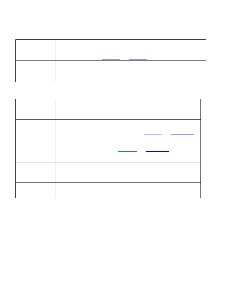
NAME
TYPE
FUNCTION
PLL_OUT
O
Transmit PLL Output. This pin can be selected to output the 1544kHz,
2048kHz, 64kHz, or 6312kHz output from the internal TX PLL or the internal
signal, TX CLOCK. See Figure 3-3 and Figure 3-4.
TCLK
I
Transmit Clock Input. A 64kHz, 1.544MHz, 2.048MHz, or 6312kHz primary
clock. May be selected by the TX PLL mux to either directly drive the transmit
section or be converted to one of the other rates prior to driving the transmit
section. See Figure 3-3 and Figure 3-4.
4.2 Transmit Side
NAME
TYPE
FUNCTION
TSER
I
Transmit Serial Data. Source of transmit data sampled on the falling edge of
(transmit timing diagram).
TS
I/O
TSYNC. When in input mode, this pin is sampled on the falling edge of TX
CLOCK (an internal signal) and a pulse at this pin will establish either frame or
multiframe boundaries for the transmit side. See Figure 3-1 and Figure 19-11.
In output mode, the pin is updated on the rising edge of TX CLOCK (an
internal signal) and can be programmed to output a frame or multiframe sync
pulse useful for aligning data. See Figure 3-1 and Figure 19-11.
TCLKO
O
Transmit Clock Output. Buffered clock that is used to clock data through the
transmit-side formatter (i.e., either TCLK or RCLK).
TPOSO
O
Transmit Positive-Data Output. In T1 or E1 mode, updated on the rising edge
of TCLKO with the bipolar data out of the transmit-side formatter. Can be
programmed to source NRZ data via the output-data format (IOCR1.0) control
bit. In 6312kHz mode, this pin is low.
TNEGO
O
Transmit Negative-Data Output. In T1 or E1 mode, updated on the rising
edge of TCLKO with the bipolar data out of the transmit-side formatter. In
6312kHz mode, this pin is low.
发布紧急采购,3分钟左右您将得到回复。
相关PDF资料
DS3105LN+
IC TIMING LINE CARD 64-LQFP
DS3106LN+
IC TIMING LINE CARD 64-LQFP
DS3231MZ+
IC RTC I2C 8SOIC
DS3231SN#T&R
IC RTC W/TCXO 16-SOIC
DS3232MZ+
IC RTC W/SRAM I2C 8SOIC
DS3232SN#T&R
IC RTC W/TCXO 20-SOIC
DS3234S#
IC RTC W/TCXO 20-SOIC
DS32C35-33#T&R
IC RTC ACCURATE I2C 3.3V 20-SOIC
相关代理商/技术参数
DS26504
制造商:Maxim Integrated Products 功能描述:T1/E1/J1 ENH BITS ELEMENT LQFP - Trays
DS26504_06
制造商:MAXIM 制造商全称:Maxim Integrated Products 功能描述:T1/E1/J1/64KCC BITS Element
DS26504DK
功能描述:网络开发工具 DS26504 Dev Kit RoHS:否 制造商:Rabbit Semiconductor 产品:Development Kits 类型:Ethernet to Wi-Fi Bridges 工具用于评估:RCM6600W 数据速率:20 Mbps, 40 Mbps 接口类型:802.11 b/g, Ethernet 工作电源电压:3.3 V
DS26504L
功能描述:计时器和支持产品 E1/T1/J1/64Kcc Bits Element RoHS:否 制造商:Micrel 类型:Standard 封装 / 箱体:SOT-23 内部定时器数量:1 电源电压-最大:18 V 电源电压-最小:2.7 V 最大功率耗散: 最大工作温度:+ 85 C 最小工作温度:- 40 C 封装:Reel
DS26504L+
功能描述:计时器和支持产品 E1/T1/J1/64Kcc Bits Element RoHS:否 制造商:Micrel 类型:Standard 封装 / 箱体:SOT-23 内部定时器数量:1 电源电压-最大:18 V 电源电压-最小:2.7 V 最大功率耗散: 最大工作温度:+ 85 C 最小工作温度:- 40 C 封装:Reel
DS26504LN
功能描述:计时器和支持产品 E1/T1/J1/64Kcc Bits Element RoHS:否 制造商:Micrel 类型:Standard 封装 / 箱体:SOT-23 内部定时器数量:1 电源电压-最大:18 V 电源电压-最小:2.7 V 最大功率耗散: 最大工作温度:+ 85 C 最小工作温度:- 40 C 封装:Reel
DS26504LN+
功能描述:计时器和支持产品 E1/T1/J1/64Kcc Bits Element RoHS:否 制造商:Micrel 类型:Standard 封装 / 箱体:SOT-23 内部定时器数量:1 电源电压-最大:18 V 电源电压-最小:2.7 V 最大功率耗散: 最大工作温度:+ 85 C 最小工作温度:- 40 C 封装:Reel
DS26504LN+T&R
制造商:Maxim Integrated Products 功能描述:T1/E1/J1 ENH BITS IC LQFP LF T&R - Tape and Reel 制造商:Maxim Integrated Products 功能描述:IC T1/E1/J1 64KCC ELEMENT 64LQFP